

RFNC-VNIIEF to Develop Semiconductor Wafer Etching System
The institute will receive 1.43 billion rubles (about $17 million) for the project.
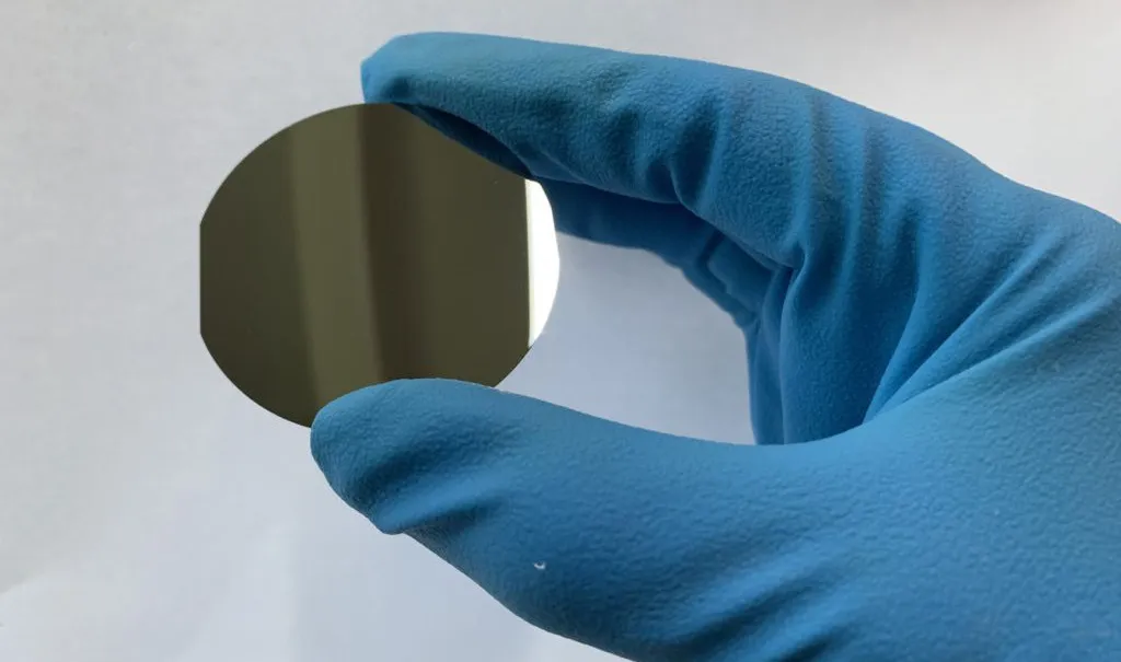
The Russian Federal Nuclear Center – All-Russian Research Institute of Experimental Physics (RFNC-VNIIEF) will develop an automated wet chemical etching system for semiconductor wafers up to 200 millimeters in diameter. The institute won a government auction and will receive 1.43 billion rubles (about $17 million) for the work.
The new equipment will be designed to chemically etch, clean, rinse and dry wafers as part of production-scale microelectronics processes. The system is intended to replace existing U.S. and Japanese equipment.
The equipment must be able to process up to 100 wafers per cycle, operate with chemicals at temperatures of up to 160 degrees Celsius (320 degrees Fahrenheit), and automatically load and unload wafers.
Etching nonuniformity across a wafer must not exceed 5%. The system must have a mean time between failures of at least 2,000 hours and a service life of at least seven years. All key components must also be manufactured in Russia.