

Russia Is Building a Complete Domestic EDA Software Stack
As part of Russia's national initiative to develop domestic electronic design automation (EDA) software, Aquarius has introduced a foundational version of a layout editor for microelectronics. The new tool is intended to become a full-featured alternative to platforms from Cadence and Synopsys, allowing chip designers to transition to Russian software with minimal disruption.
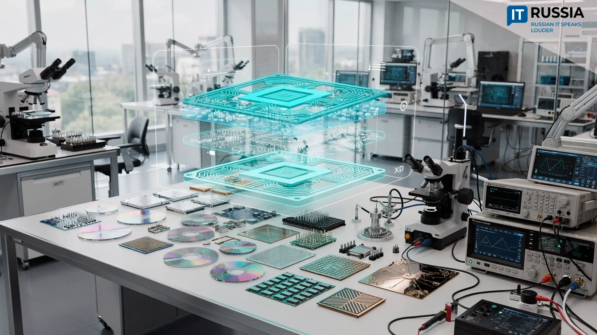
Aquarius is participating in a government program to develop Russian electronic design automation (EDA) systems for the microelectronics industry. The company's new layout editor is intended to evolve into a full-featured alternative to software from Cadence and Synopsys, allowing engineers to migrate to domestic design tools without major obstacles.
The work is being carried out under a contract from Russia's Ministry of Industry and Trade as part of the roadmap "Sistemy avtomatizirovannogo proyektirovaniya mikroelektroniki do 2030 goda" (Microelectronics Electronic Design Automation Systems Through 2030). The general contractor is JSC Research and Production Association Critical Information Systems (JSC NPO KIS), part of Rosatom (State Atomic Energy Corporation Rosatom).
Since 2025, Aquarius has been developing one of the EDA platform's core modules while also testing the integrated product being built in cooperation with other participants in the program. That approach allows the company to influence not only the quality of individual components but also the reliability of the overall platform. The development effort is centered on end-user needs: technical specifications provide the starting point, while additional functionality and carefully designed ergonomics are built on top of that foundation. This approach makes it possible to deliver a commercially mature product that is practical for engineers and capable of competing with leading international platforms. The team's immediate objective is to ensure compatibility between the layout editor, other software modules, component libraries, and the parameters of Russian semiconductor manufacturing processes.
Three Stages of Russia's Microelectronics Strategy
A complete EDA environment requires tightly integrated simulation, verification, and photomask preparation tools. That broader objective is being addressed at the national level. In April 2026, the Ministry of Industry and Trade allocated approximately RUB 943 million (more than USD 12 million) to develop software supporting semiconductor process technologies of 90 nanometers and above.
The software suite under development will include modules for data import, layout visualization and inspection, layout drafting, photomask assembly, and other engineering functions. Together, these components point to plans for a fully self-contained semiconductor design workflow in which the software can operate without a network connection. The ministry has also established more ambitious long-term targets. By 2030, Russia aims to deliver EDA software supporting 28 nm chip design, followed by software for 16 nm processor development between 2030 and 2032.
From RF ICs to Photonics: A Complete Russian EDA Portfolio
The roadmap "Sistemy avtomatizirovannogo proyektirovaniya mikroelektroniki do 2030 goda" (Microelectronics Electronic Design Automation Systems Through 2030), adopted in 2024, spans a broad range of technologies. Research and development spending under the program is estimated at RUB 54.6 billion (more than USD 700 million).
Aquarius is one of dozens of companies and research organizations participating in the Ministry of Industry and Trade's initiative. One of the flagship projects within the modular ecosystem is a digital very-large-scale integration (VLSI) EDA platform covering the complete integrated circuit design flow, including logic synthesis, functional verification, physical verification, placement, and routing. The project is being developed by the National Research University of Electronic Technology (MIET) and its innovation center (MNTC MIET), together with Lomonosov Moscow State University, the Ivannikov Institute for System Programming of the Russian Academy of Sciences, and the companies Eremex, Alfachip, and NPK TC. NM-Tech is developing advanced tools for characterization and parameterization of standard-cell libraries supporting process technologies from 28 nm to 90 nm. Researchers at the Moscow Institute of Physics and Technology are developing software for advanced semiconductor packaging and three-dimensional assemblies. Tomsk State University of Control Systems and Radioelectronics, together with the National Computer Corporation (NCC), is creating Russia's first EDA platform for RF integrated circuits, antennas, and microwave devices. That capability is particularly important for telecommunications equipment, radar systems, and space technologies. A baseline version with essential functionality is scheduled for completion by the end of 2026, followed by a next-generation platform by 2030 designed to compete directly with international products.

100 EDA Platforms by 2030
Together, these initiatives are forming a modular Russian EDA ecosystem. Between 2021 and 2024, the Ministry of Industry and Trade's roadmap produced 58 software modules. Another 49 are scheduled for deployment by the end of this year. By 2028, the program aims to deliver a total of 216 modules covering every stage of integrated circuit design.
Successful implementation of the national program would establish a fully independent semiconductor design workflow while steadily replacing imported software. By 2030, Russia plans to develop approximately 100 different EDA platforms. Sales are projected to reach about 2,600 software licenses, generating total revenue of RUB 7.2 billion (approximately USD 93 million), including RUB 3.6 billion (approximately USD 46 million) from integrated circuit design software. That would allow Russia not only to meet domestic demand but also to offer competitive EDA platforms to partner countries.