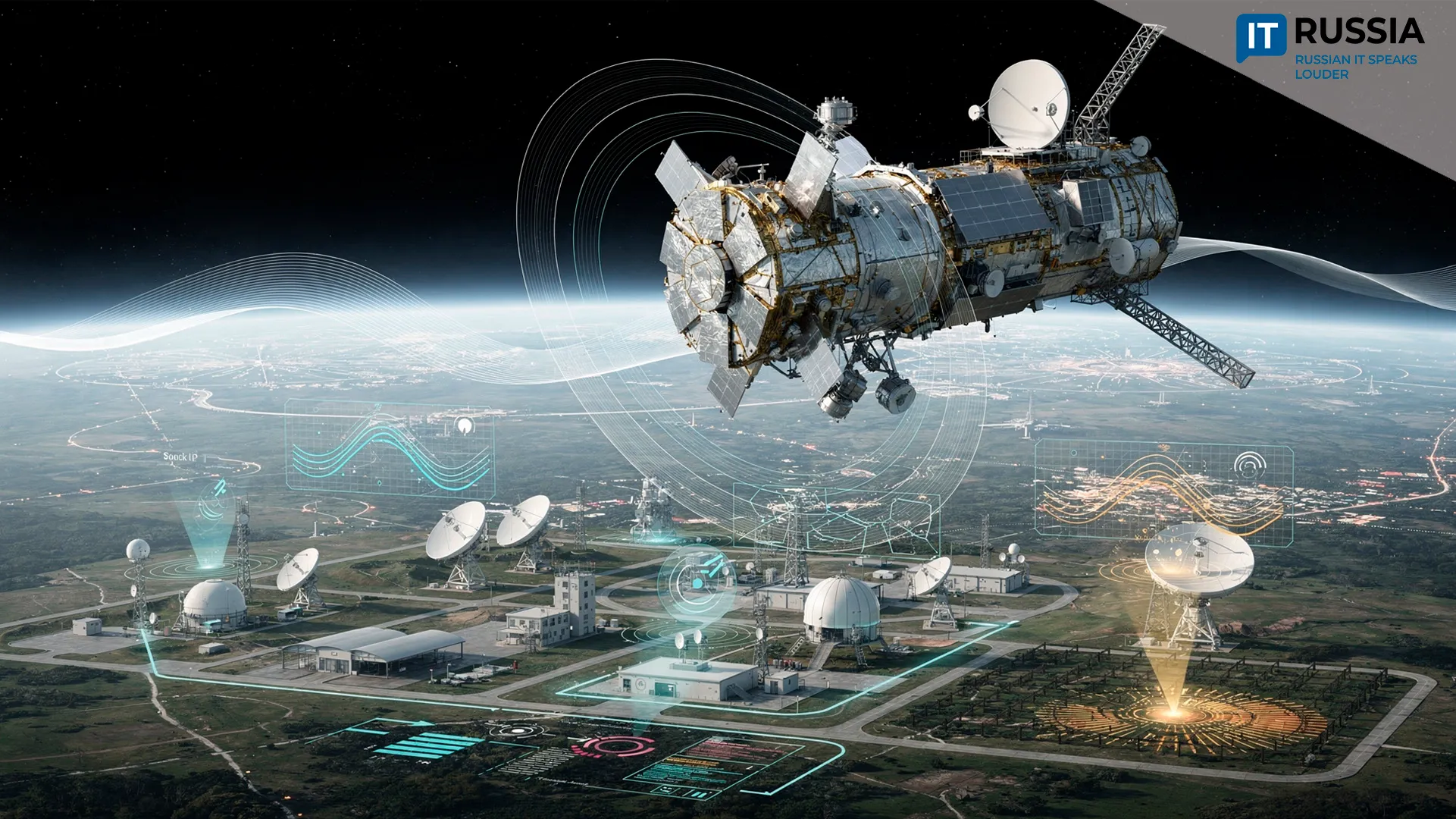
Russian Cosmonauts Grow Semiconductor Crystal Films on the ISS
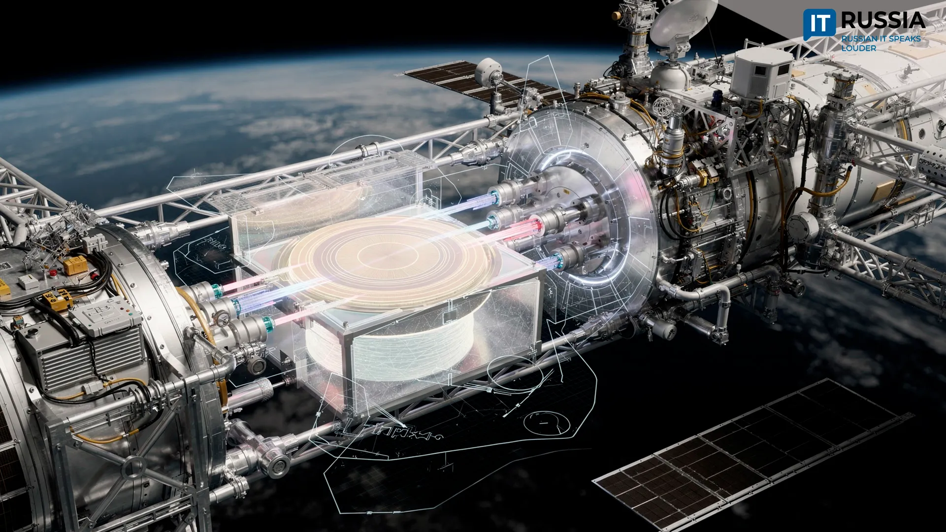
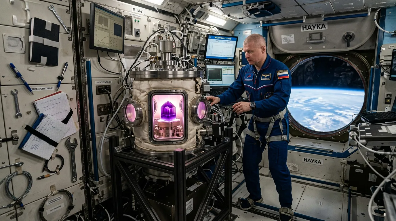
On the Russian segment of the ISS, the second session of the “Ekran-M” experiment has been conducted to produce ultra-pure semiconductor crystals. The work focuses on growing structures based on gallium arsenide in the vacuum of space and microgravity.
Technological development on Earth is pushing a global shift toward moving vacuum-based processes into space, where natural conditions eliminate the need for massive infrastructure. On Earth, ultra-high vacuum systems are complex, expensive, and can weigh several tons.
During a live broadcast of the experiment, observers could see cosmonauts calmly handling a compact vacuum unit, highlighting how space fundamentally changes the scale of such technologies.
Unique Experiment on the ISS
The second session of the Ekran-M (Molecular Screen) experiment has been completed on the Russian segment of the International Space Station. In the vacuum and microgravity environment, cosmonauts are growing ultra-pure semiconductor structures based on gallium arsenide, a material critical for microelectronics, photonics, and next-generation energy systems.
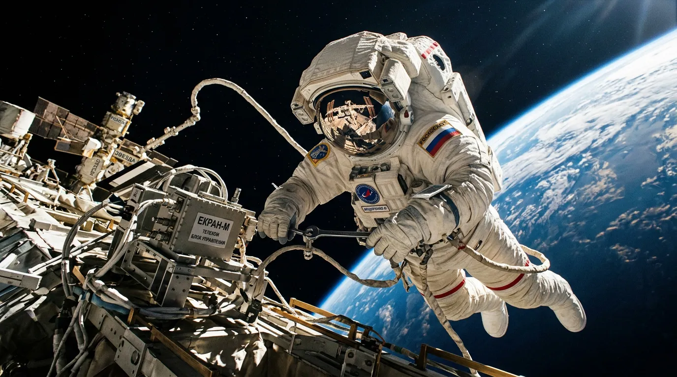
The experimental hardware was installed outside the ISS in 2025 by Roscosmos cosmonauts Sergey Ryzhikov and Alexey Zubritsky. Placing the system outside the station enables semiconductor growth under near-ideal high-vacuum and microgravity conditions using molecular beam epitaxy.
The session was conducted manually, as sensor behavior required intervention by the crew. Developers from RKK Energia and the Russian Academy of Sciences note that this scenario was anticipated in the system design. It is not a malfunction, but part of validating the technology’s robustness.
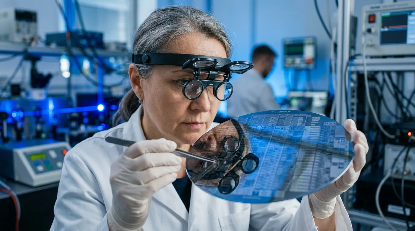
The unit delivered to the ISS in 2025 has already produced the first near-perfect crystal structures grown in open space. By March 2026, the project has moved beyond demonstration into a phase of systematic validation. Comparison of space-grown semiconductor materials with terrestrial counterparts will be carried out at the Institute of Semiconductor Physics of the Siberian Branch of the Russian Academy of Sciences.
Russian researchers already have extensive experience in growing and studying epitaxial materials, including gallium arsenide. They have established synthesis and analysis methods, their own equipment, and access to a large body of international research, ensuring a comprehensive evaluation of the structures produced in space.
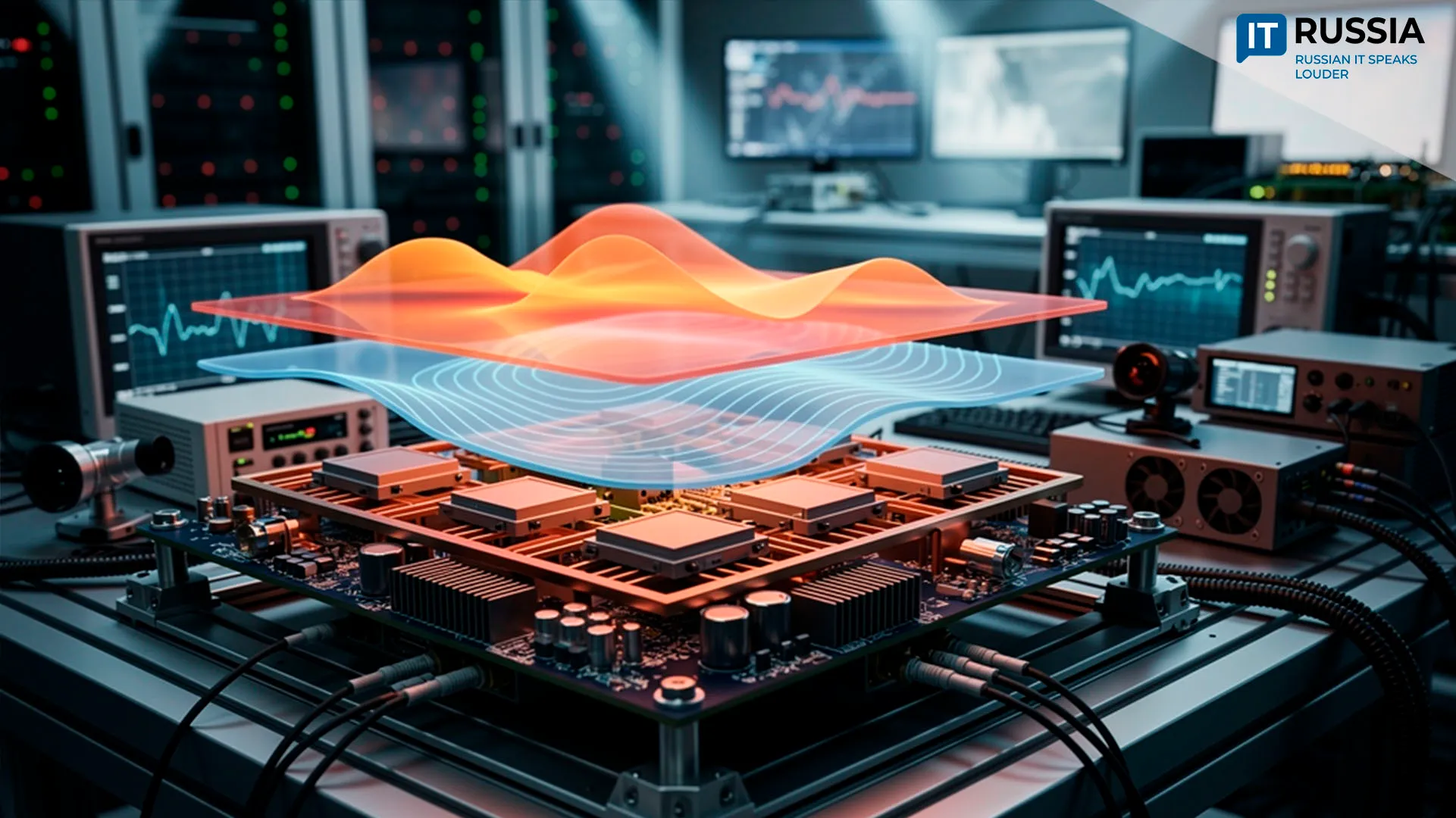
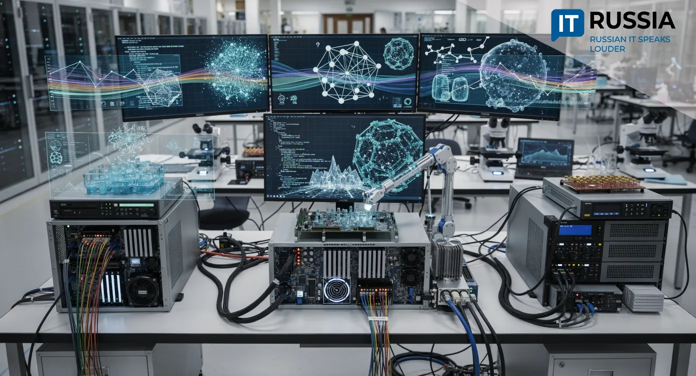
On Earth, growing gallium arsenide is constrained by impurities and crystal defects caused by gravity and convection. In microgravity, these effects are minimized, theoretically enabling structures with unprecedented purity and uniformity. Ekran-M uses molecular beam epitaxy, a technique that assembles crystals layer by layer at the atomic scale. The experiment is not only a scientific study, but also a test of a new production platform.
Technological Sovereignty: From Orbit to Earth Applications
For Russia’s IT sector and defense industry, the project extends beyond fundamental science. Ekran-M is emerging as part of a broader strategy for technological sovereignty. In the long term, it supports the creation of a domestic component base for communications, satellite systems, sensors, and power electronics. The project links academic research, space infrastructure, and applied industry, contributing to more reliable telecom systems, navigation services, and specialized electronics.
Space as a Manufacturing Environment
The Russian experiment is unfolding amid growing global interest in orbital manufacturing. US-based Varda Space is developing commercial models for producing pharmaceuticals and materials in microgravity. However, Ekran-M remains the only active program focused on growing semiconductor structures using molecular beam epitaxy in open space. Its success could support the case for next-generation automated orbital laboratories and position Russia as a leader in space-based materials science.
From Experiment to Industry
In the long term, data obtained from the experiment could support the deployment of semiconductor manufacturing in orbit, including the production of photosensitive materials for solar panels. Such production requires ultra-pure conditions and involves toxic compounds. In space, waste is naturally expelled from the chamber without harming the environment, unlike on Earth.
As humanity expands its presence in space, the need for off-Earth production of materials and components for orbital operations and deep-space missions will become inevitable. The Russian experiment represents one of the first steps in this direction. The experience gained in designing and operating space-based technological equipment will inform future developments.